Protection Devices and Circuitry
While MOSFETs are very rugged devices from a current standpoint, like
all semiconductors, they are subject to immediate damage or destruction if
the voltage ratings of the device are exceeded. The most common failure modes
of MOSFETs in class E transmitters are gate puncture due to voltage spikes at
the gates of the MOSFET, and drain-source (high voltage) breakdown.
Gate Protection
Gate voltage spikes are generally a result of gate overdrive. This is usually
remedied by using a stable driver, and by adding protection devices to the
gate circuit.
With Digital gate drive, assuming the drivers are fed by a good, reliable
power supply, the drivers themselves typically protect the gates of the
MOSFETs they are driving.
Parasitic Oscillations and Drain Protection
The primary cause of drain source failure is a parasitic oscillation in the
class E RF amplifier. Another very common cause is related to poor or failing shunt capacitors (capacitors
usually lose value when heated - some will momentarily fail) allowing large
voltages to occur during MOSFET turn off, which would otherwise not be present if the capacitor
were working properly. Shunt capacitor problems can be hard to find, and are
generally intermittent in nature. Use high quality, high current shunt
capacitors.
Parasitic oscillations come about when the MOSFETs are allowed to
operate in their analog (or linear) region for a long enough time for a
parasitic oscillation to get going. This region exists between the
MOSFET gate threshold voltage and saturation voltage. MOSFETs have extremely
high voltage gain, combined with very high capacitances, which makes the
devices very prone to parasitics unless steps are taken to prevent them. Using
Digital Gate Drive, and using good construction practices (short leads,
neat layout, etc.) will go along way to ensure that the class E amplifier is
stable.
In
audio circuits, and switching power supplies operating below 1mHz, it is usually
sufficient to insert a resistor between the gate of each MOSFET and any other
components, to stablize the MOSFET against parasitics. In class E amplifiers
operating above 2 mHz, this is not always practical. Even a small resistance in series
with the gate will significantly reduce the gate drive, and will slow the
rise and fall times of the gate waveform.
The best way to prevent parasitics is to use a gate driver circuit
that guarantees the MOSFET gates are actively held in either the ON or OFF
state at all times. The gates must never be allowed to "float" or be subject
to a high impedance driving source. If the gate drive drops under modulation,
you may also be in danger of allowing the MOSFETs to operate in their linear
range, giving rise to possible parasitics. The most fool proof driver for a
MOSFET is a driver IC connected directly to the gate, with short leads and good
grounding and bypassing.
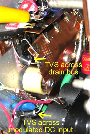
You can protect the drains from the possibility of overvoltage
caused by parasitics and other anomalies by using a TVS across
the drain bus. A couple of 1.5KE540A TVS devices, connected from the drain bus to the
source bus has proven effective in helping to reduce or eliminate voltage spikes
that would otherwise cause device failure.
The modulated DC input to the RF amplifier should also be protected with
130V (1.5KE130A) TVS devices. This will prevent high voltage spikes caused by
inductance in the modulator circuitry from reaching the RF amplifier. These
devices should be located right at the RF amplifier, one for each module.
|